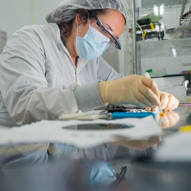
Optical and X-ray techniques are powerful ways to characterize semiconductor thin films. They can be used to measure film thickness, purity and crystalline quality, and for compositional analysis. Modern techniques are fast, turn-key, and generally non-destructive, allowing for rapid assessment of material properties. This course describes the fundamentals of optical and X-ray characterization and provides real-world examples of how they are used in semiconductor manufacturing.
Class Deals by MOOC List - Click here and see Coursera's Active Discounts, Deals, and Promo Codes.
This course is part of the Semiconductor Characterization Specialization.
What you'll learn
- Describe the use of light to measure the thickness and refractive index of thin transparent films.
- Explain how light is absorbed and emitted by semiconductors.
- Explain the advantages and limitations of optical and X-ray characterization.
Syllabus
Course Introduction
Optical and X-ray techniques are powerful ways to characterize semiconductor thin films. They can be used to measure film thickness, purity and crystalline quality, and for compositional analysis. Modern techniques are fast, turn-key, and generally non-destructive, allowing for rapid assessment of material properties. This course describes the fundamentals of optical and X-ray characterization and provides real-world examples of how they are used in semiconductor manufacturing.
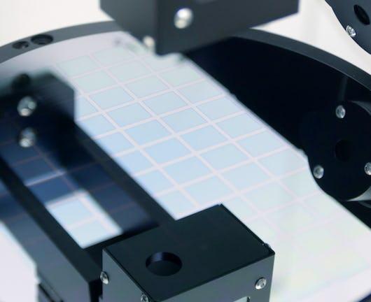
Week 5.1: Reflectance Spectroscopy
This week introduces the concept of reflectance spectroscopy: a rapid, convenient, and non-destructive technique for measuring the thickness of transparent materials.
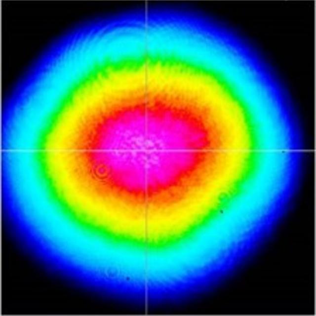
Week 5.2: Ellipsometry
This week, you will learn about ellipsometry, a powerful technique that allows us to extract the thickness and refractive index of transparent layers as thin as a few nanometers.
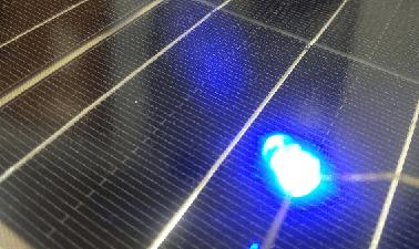
Week 5.3: Photoluminescence
This week, you will learn about photoluminescence.
Week 5.4: Electron Microprobe X-Ray Analysis
This week, you will learn about electron microprobe X-ray analysis.
Week 5.5: Course Wrap-up and Project
This week, you will complete a case study to assess your ability to analyze electron microprobe x-ray images to determine the constituent elements in a 40 nm MOSFET.