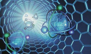
The aim of the course is a basic acquaintance with the concepts and approaches used in the field of nanomaterials design, fabrication and analysis. The course examines the physical basis of modern nanotechnology from the standpoint of semiconductor physics and quantum mechanics. The range of issues covered includes nanosystems classification by dimension, consideration of "bottom-up" and "from top down" approaches, examples of nanomaterials and nanosystems properties changes, the basis of practical device fabrication technologies for electronics, microwave photonics and photovoltaics, as well as the most important techniques for nanomaterial and device characterization.
Class Deals by MOOC List - Click here and see EdX's Active Discounts, Deals, and Promo Codes.
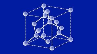
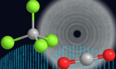
The basics of physics and technology of nanomaterials and nanosystems are overviewed in the course. The terminology and notions are introduced. The changes in the main properties of semiconductors and metals due to decrease of their size are discussed towards the electronic and optoelectronic applications and modern compound semiconductor materials. Starting from the objects description and mail physical properties peculiarities we move to basics of material and device nanofabrication, ending with nanosystem characterization techniques. Fabrication nanotechnology of the microwave compound semiconductor heterostructure devices for electronics and photonics are outlined.
What you'll learn
- Concepts and approaches used in the field of nanomaterials design, fabrication and analysis
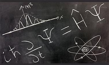
- The physical basis of modern nanotechnology from the standpoint of semiconductor physics and quantum mechanics
- Nanosystems classification by dimension, consideration of "bottom-up" and "from top down" approaches
- The basis of practical device fabrication technologies for electronics, microwave photonics and photovoltaics
Syllabus
Week 1. The size and dimensionality of nanosystems
What is nano and why it is so helpful?
The size and dimensionality of nanosystems
Week 2. Nanosystems and their basic properties
2D Quantum heterostructure design and applications
Low-dimensional nanosystems and their properties
Week 3. Self-organization and self-assembly technology
Self-organization and self-assembly technology
Week 4. Directional nanostructuring techniques
Directional nanostructuring techniques
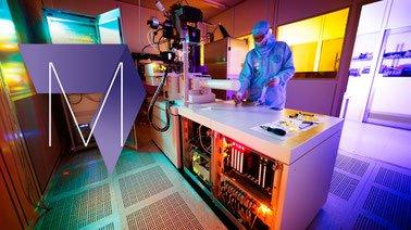
Week 5. Nanofabrication of compound semiconductor devices
Nanofabrication of compound semiconductor devices
Week 6. Nanotechnology in microwave electronics and photonics devices
Nanotechnology in microwave electronics and photonics devices
Week 7. Methods of nanostructure material characterization
Methods of nanostructure material characterization
Week 8. Electrical and optical characterization techniques for nanosystems
Electrical and optical characterization techniques for nanosystems