This course can also be taken for academic credit as ECEA 5722, part of CU Boulder’s Master of Science in Electrical Engineering. This course is primarily aimed at first year graduate students interested in engineering or science, along with professionals with an interest in power electronics and semiconductor devices .
Class Deals by MOOC List - Click here and see Coursera's Active Discounts, Deals, and Promo Codes.
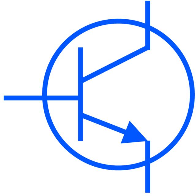
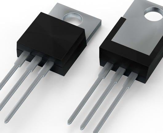
It is the second course in the "Semiconductor Power Device" specialization that focusses on diodes, MOSFETs, IGBT but also covers legacy devices (BJTs, Thyristors and TRIACS) as well as state-of-the-art devices such as silicon carbide (SiC) Schottky diodes and MOSFETs as well as Gallium Nitride (GaN) HEMTs. The specialization provides an overview of devices, the physics background needed to understand the device operation, the construction of a device circuit model from a physical device model and a description of the device fabrication technology including packaging.
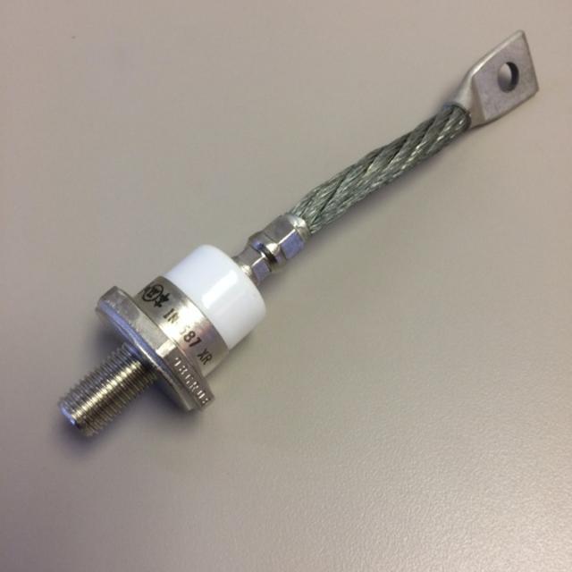
This second course provides a more detailed description of high-voltage Schottky and p-n diodes, starting with the semiconductor physics background needed to analyze both types of diodes. The main properties of crystalline semiconductors are presented that lead to the calculation of carrier densities and carrier currents, resulting in the drift-diffusion model for the semiconductors of interest. Next are a close look at Schottky diodes followed by p-n diodes, with a focus on the key figures of merit including the on-resistance, breakdown voltage and diode capacitance. For each diode, the analysis is then linked to the corresponding SPICE model. Finally, the power diode losses - both on-state losses and switching losses - are examined in a convertor circuit, including a comparison of silicon p-n diodes and 4H-SiC Schottky diodes.
Learning objectives:
• Provide students with a detailed understanding of High-Voltage Schottky and p-n diodes.
• Students will be able to calculate key diode parameters based on their physical structure.
• Students will be able to construct SPICE models for Schottky and p-n diodes.
What You Will Learn
· Gain a detailed understanding of Schottky and p-n diodes.
· Calculate key diode parameters based on their physical structure.
Syllabus
WEEK 1
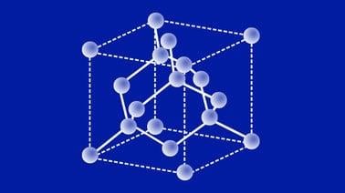
Semiconductor physics background
In this module, you will learn about semiconductors: the material used to make power semiconductor devices. Specifically you will learn: a) types of semiconductors that are of interest and their crystal structure, b) band structure of relevant semiconductors, c) How to calculate the majority and minority carrier density in a semiconductor, d) How to deal with electron and hole drift and diffusion, and e) How to deal with carrier generation and recombination. This module closes with the drift-diffusion model, the cornerstone of any semiconductor device analysis.
WEEK 2
Schottky diodes
In this module, you will learn about the simplest semiconductor device, a Schottky diode, which consists of a metal-semiconductor junction. You will apply the drift-diffusion model, solving Gauss' law leading to the depletion layer width, the maximum electric field and capacitance versus voltage relation. Next is the derivation of the Schottky diode current. The analysis of diode breakdown at high voltage is included as well, as is the construction of a SPICE model including parasitic elements.
WEEK 3
p-n Diodes
In this module, you will learn how to analyze a p-n diode and how it differs from a Schottky diode. Specific items of interest are: a) The capacitance versus voltage relation, b) The diode current, including minority carrier injection under forward bias, c) The minority carrier charge and its effect on switching losses, and d) The construction of a p-n diode SPICE model including parasitic circuit elements.
WEEK 4
Power diode losses
In this module, you will learn about the trade-off between diode losses and breakdown voltage including: a) The diode resistance and its relation to the breakdown voltage, b) The switching losses and relation to diode capacitance and minority charge storage, and c) A detailed comparison of SiC Schottky and silicon p-n diodes.