Semiconductor Packaging Manufacturing (Coursera)

Semiconductor Packaging Manufacturing (Coursera)

This course will provide information on the various stages of semiconductor package manufacturing, including sort, assembly, and final test. In addition, we will also describe how to select, build, and test the packages with the die and other components to ensure the quality of the package and total assembly performance.

Class Deals by MOOC List - Click here and see Coursera's Active Discounts, Deals, and Promo Codes.

We will also discuss the role of Process Control Systems in semiconductor manufacturing as they relate to quality testing. Specifically, we will explore how Process Control Systems can help identify and correct process problems that cause variation and quality issues. Finally, we also demonstrate how to use control charts to monitor the process performance. These can assist in decision-making, specifically when to take action to improve the process.
Course 2 of 3 in the Semiconductor Packaging Specialization.

What You Will Learn

  • Learn about the various stages of semiconductor package manufacturing.
  • The role of Process Control Systems in semiconductor manufacturing.
  • How Process control Systems can help identify and correct process problems.
  • How to use control charts to monitor process performance.

Syllabus

WEEK 1
Welcome
Welcome to Semiconductor Packaging Manufacturing, where we discuss the various stages of semiconductor package manufacturing, including sort, assembly, and final test. In addition, we will also describe how to select, build, and test the packages with the die and other components to ensure the quality of the package and total assembly performance. We will also discuss the role of Process Control Systems in semiconductor manufacturing as they relate to quality testing. Specifically, we will explore how Process Control Systems can help identify and correct process problems that cause variation and quality issues. Finally, we also demonstrate how to use control charts to monitor the process performance. These can assist in decision-making, specifically when to take action to improve the process.

WEEK 2
Introduction to Semiconductor Package Manufacturing 1
In this module you will have an opportunity to view a lecture video by Principal Engineer, Dr. Mitul Modi from Intel as he discusses semiconductor package manufacturing. He will explain how semiconductor packaging is a complex process and discuss the three primary phases: sort, assembly, and final test.

WEEK 3
Introduction to Semiconductor Package Manufacturing 2
In this module you will have an opportunity to view a lecture video by Principal Engineer, Dr. Mitul Modi from Intel as he discusses process flows for different types of semiconductor packages. He will explain how most process flows consist of three basic steps: sort, assembly, and final test. You will learn the details of how these steps vary depending on the package type. Mitul will give examples of process flows for BGA, LGA, 3D stacked LGA, and Stacked Hybrid packages. He will also mention that there are many more possible scenarios for process flows in semiconductor packaging.

WEEK 4
Assembly Part 1
In this module you will have an opportunity to view a lecture video by Principal Engineer, Dr. Mitul Modi from Intel as he discusses the assembly process of semiconductor packaging and their purposes. He explains how the die is prepared, attached to a substrate, and the importance of the epoxy process. He also discuss other assembly techniques for each of these steps.

WEEK 5
Assembly Part 2
In this module you will have an opportunity to view a lecture video by Principal Engineer, Dr. Mitul Modi from Intel as he discusses the different types of assembly steps in semiconductor packaging and their purposes. You will learn about the optional steps of IHS attach and ball attach, and how they improve the performance and reliability of the packages.

WEEK 6
Test and Finish
In this module you will have an opportunity to view a lecture video by Principal Engineer, Dr. Mitul Modi from Intel as he discusses the test and final stages of semiconductor packaging and their importance. Mitul describes how sort, burn-in, test and finish operations ensure the quality, functionality and reliability of the packages before they are delivered to the customer.

WEEK 7
Process Control Systems (PCS)
In this module you will have an opportunity to view a lecture video by Principal Engineer, Dr. Mitul Modi from Intel as he discusses the role and benefits of Process Control Systems (PCS) in semiconductor manufacturing. He will explain how PCS can detect and correct process problems that cause variation and quality issues. He will also define the concepts of targets, variation, common and special causes, control limits, and stability. Mitul will demonstrate how to use control charts to monitor the process performance and to decide when to take action to improve the process.

WEEK 8
Semiconductor Packaging Manufacturing Course Summary
In conclusion of Introduction to Semiconductor Packaging, we would like to summarize the main takeaways. We started by sharing various aspects of nanoelectronics, transistor action, reliability, and customer ease of use. Then, we explored how Moore’s Law and market use conditions affect the packages' reliability needs and the materials/design choices. At the end, we saw how the common footprint of a motherboard or socket determines a package's substrate level interconnect. Thank you for joining us.
Go to Class
MOOC List is learner-supported. When you buy through links on our site, we may earn an affiliate commission.

Related Courses

Introduction to solar cells (Coursera) Coursera
Technical University of Denmark - DTU

Introduction to solar cells (Coursera)

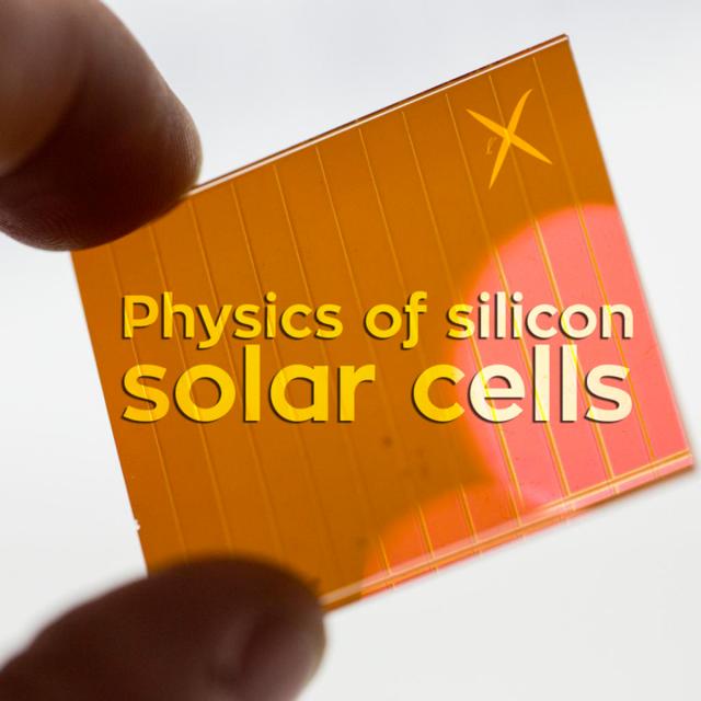
How do solar cells work, why do we need, and how can we measure their efficiency? These are just some of the questions Introduction to solar cells tackles. Whether you are looking for general insight in this green technology or your ambition is to pursue a career in solar, “Introduction to Solar Cells” is an excellent starting point. The course is a tour through the fundamental disciplines including solar cell history, why we need solar energy, how solar cells produce power, and how they work. During the course we cover mono- and multi-crystalline solar cells, thin film solar cells, and new emerging technologies.

Jul 27th 2026
5-12 Weeks
Perspectives in Digital Transformation: Manufacturing (Coursera) Coursera
Inter-American Development Bank - IDB

Perspectives in Digital Transformation: Manufacturing (Coursera)

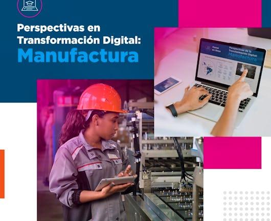
Are you interested in learning how Digital Transformation is driving the manufacturing sector in Latin America and the Caribbean? This course will help you identify challenges and opportunities that digitalization can offer in the industry. Along with specialists from BID Invest and the private sector, you will learn firsthand about the tools and best practices that illustrate the potential of digital solutions, with a cross-cutting focus on sustainability.

Aug 3rd 2026
4 Weeks
Introduction to Semiconductor Devices 2 (Coursera) Coursera
Korea Advanced Institute of Science and Technology - KAIST

Introduction to Semiconductor Devices 2 (Coursera)

This course aims to provide a general understanding of semiconductor devices. This coures covers the Metal-Semiconductor Contact, Metal-Oxide-Semiconductor (MOS) capapcitor, Metal-Oxide-Semiconductor Field Effect Transistors(MOSFETs), CMOS, Metal-Semiconductor Field Effect Transistors(MESFETs), Memory and Bipolar Junction Transistor (BJT) to improve the overall knowledge of semiconductor industry.

Jul 27th 2026
5-12 Weeks
Electrical Characterization: MOSFETs (Coursera) Coursera
Arizona State University

Electrical Characterization: MOSFETs (Coursera)

MOSFET transistor switches are the workhorse of semiconductor-based electronics. In this course, we begin with MOS capacitors and see how to extract the oxide charge density, which is important for controlling the MOSFET threshold voltage. We then review MOSFET electrical characteristics and see how current-voltage measurements are used to determine the threshold voltage. The course project uses real-world data to extract the threshold voltage of a 40 nm gate length MOSFET designed for 5G radio frequency integrated circuits.

Aug 3rd 2026
5-12 Weeks
Cyber Security in Manufacturing (Coursera) Coursera
University at Buffalo,The State University of New York

Cyber Security in Manufacturing (Coursera)

The nature of digital manufacturing and design (DM&D), and its heavy reliance on creating a digital thread of product and process data and information, makes it a prime target for hackers and counterfeiters. This course will introduce students to why creating a strong and secure infrastructure should be of paramount concern for anyone operating in the DM&D domain, and measures that can be employed to protect operational technologies, systems and resources.

Jul 27th 2026
4 Weeks
Optical and X-Ray Characterization (Coursera) Coursera
Arizona State University

Optical and X-Ray Characterization (Coursera)

Optical and X-ray techniques are powerful ways to characterize semiconductor thin films. They can be used to measure film thickness, purity and crystalline quality, and for compositional analysis. Modern techniques are fast, turn-key, and generally non-destructive, allowing for rapid assessment of material properties. This course describes the fundamentals of optical and X-ray characterization and provides real-world examples of how they are used in semiconductor manufacturing.

Aug 3rd 2026
5-12 Weeks
Advanced Semiconductor Packaging (Coursera) Coursera
Arizona State University

Advanced Semiconductor Packaging (Coursera)

Throughout this course, you will be introduced to Pathway for Assembly and Packaging technologies for 7-nanometer silicon feature sizes and beyond. The course will present the evolution and impact of packaging on product performance and innovation. Specifically, we highlight how packaging has enabled better products via the use of heterogeneous integration by improving the interconnects for thermal management and signal integrity.

Jul 27th 2026
5-12 Weeks
Advanced Manufacturing Enterprise (Coursera) Coursera
University at Buffalo,The State University of New York

Advanced Manufacturing Enterprise (Coursera)

Enterprises that seek to become proficient in advanced manufacturing must incorporate manufacturing management tools and integrate data throughout the supply chain to be successful. This course will make students aware of what a digitally connected enterprise is, as they learn about the operational complexity of enterprises, business process optimization and the concept of an integrated product-process-value chain.

Jul 27th 2026
4 Weeks
Factory Automation: Shaping the Future of Manufacturing (Coursera) Coursera
Starweaver

Factory Automation: Shaping the Future of Manufacturing (Coursera)

This course provides a comprehensive understanding of factory automation, covering foundational concepts to practical applications. Participants explore the evolution of automation technology, including robotics and control systems, witnessing its role in optimizing production processes and enhancing productivity. Through real-world case studies, they learn how automation improves efficiency, safety, and innovation in manufacturing.

Aug 17th 2026
4 Weeks
3D Printing Applications (Coursera) Coursera
University of Illinois at Urbana-Champaign

3D Printing Applications (Coursera)

This course will help you understand how 3D printing is being applied across a number of domains, including design, manufacturing, and retailing. It will also demonstrate the special capabilities of 3D printing such as customization, self-assembly, and the ability to print complex objects. In addition to business applications, this course will also examine how individuals, including those in developing countries, are using this technology to create solutions to the problems they face.

Aug 3rd 2026
4 Weeks
Electron and Ion Beam Characterization (Coursera) Coursera
Arizona State University

Electron and Ion Beam Characterization (Coursera)

Electron and ion beams are widely used for both qualitative and quantitative analysis of semiconductor materials and devices. They can be used to image structures with sub-nm resolution and to provide information about elemental composition and dopant concentration. This course describes the fundamentals of electron and ion beam characterization and includes a project that analyzes the surface roughness of a solar cell.

Aug 3rd 2026
5-12 Weeks