MOOC List is learner-supported. When you buy through links on our site, we may earn an affiliate commission.
MOOC List is learner-supported. When you buy through links on our site, we may earn an affiliate commission.
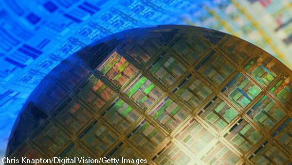
This class focuses on the major design tools used in the creation of an Application Specific Integrated Circuit (ASIC) or System on Chip (SoC) design. Our focus in this part of the course is on the key logical and geometric representations that make it possible to map from logic to layout, and in particular, to place, route, and evaluate the timing of large logic networks. Our goal is for students to understand how the tools themselves work, at the level of their fundamental algorithms and data structures. Topics covered will include: technology mapping, timing analysis, and ASIC placement and routing.
Recommended Background:
Programming experience (C, C++, Java, Python, etc.) and basic knowledge of data structures and algorithms (especially recursive algorithms). An understanding of basic digital design: Boolean algebra, Kmaps, gates and flip flops, finite state machine design. Linear algebra and calculus at the level of a junior or senior in engineering. Elementary knowledge of RC linear circuits (at the level of an introductory physics class).
You should complete the VLSI CAD Part I: Logic course before beginning this course.
Syllabus
WEEK 1
Orientation
In this module you will become familiar with the course and our learning environment. The orientation will also help you obtain the technical skills required for the course.
ASIC Placement
In this second part of our course, we will talk about geometry. We will begin with an overview of the ASIC layout process, and discuss the role of technology libraries, tech mapping (a topic we delay until the following week, to let those who want to do the Placer programming assignment have more time), and placement and routing. In this set of lectures, we focus on the placement process itself: you have a million gates from the result of synthesis and map, so, where do they go? This process is called “placement”, and we describe an iterative method, and a mathematical optimization method, that can each do very large placement tasks.
WEEK 2
Technology Mapping
Technology Mapping! We omitted one critical step between logic and layout, the process of translating the output of synthesis -- which is NOT real gates in your technology library -- into real logic gates. The Tech Mapper performs this important step, and it is a surprisingly elegant algorithm involving recursive covering of a tree. Another place where knowing some practical computer science comes to the rescue in VLSI CAD.
WEEK 3
ASIC Routing
Routing! You put a few million gates on the surface of the chip in some sensible way. What's next? Create the wires to connect them. We focus on Maze Routing, which is a classical and powerful technique with the virtue that one can "add" much sophisticated functionality on top of a rather simple core algorithm. This is also the topic for final (optional) programming assignment. Yes, if you choose, you get to route pieces of the industrial benchmarks we had you place in the placer software assignment.
WEEK 4
Timing Analysis
You synthesized it. You mapped it. You placed it. You routed it. Now what? HOW FAST DOES IT GO? Oh, we need some new models, to talk about how TIMING works. Delay through logic gates and big networks of gates. New numbers to understand: ATs, RATs, SLACKS, etc. And some electrical details (minimal) to figure out how delays happen through the physical geometry of physical routed wires. All together this is the stuff of Static Timing Analysis (STA), which is a huge and important final "sign off" step in real ASIC design.
WEEK 5
Final Exam
There is no new content this week. Instead, you should focus on finishing the last problem set and completing the Final Exam.
MOOC List is learner-supported. When you buy through links on our site, we may earn an affiliate commission.
MOOC List is learner-supported. When you buy through links on our site, we may earn an affiliate commission.